


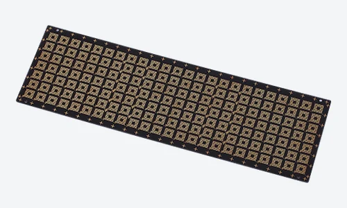
The short version: there is no universal surface finish for ceramic substrates. What this surface can be was already narrowed the moment you picked a metallisation system — and on the same board, pads destined for solder and pads destined for wire bonding want opposite things. A drawing that says only "surface finish: ENIG" hands the fabricator an incomplete input. It does not say which pads get soldered, which get bonded, and which should never be wetted at all.
1. Why FR-4 surface finish conclusions do not transfer
On FR-4, the finish is a fairly independent back-end choice. Plated copper underneath, solder mask on top, openings expose copper, and the whole board gets one treatment. Comparing finishes against each other works because the premises are shared: copper below, boundaries defined by mask.
Ceramic removes both premises.
First, what is underneath is not necessarily plated copper. Ceramic metallisation follows several genuinely different routes: printing a metal paste and firing it, sputtering a seed layer and plating it up, or bonding a copper foil directly to the ceramic. The resulting metal surfaces differ in composition, grain condition, roughness and in what wet processing they tolerate. A fired paste surface and an electroplated copper surface are not the same object to be treated.
Second, there is not necessarily solder mask on top. Ceramic substrates frequently ship without mask, particularly where heat has to leave, where operating temperature is high, or where bonding is planned. No mask means no opening boundary. Where solder flows and where it stops is then set not by printed ink but by the geometry of the metallisation itself.
Together these mean: on ceramic, surface finish is not a field you fill in last. It is a set of decisions tied to the metallisation system and to the assembly method. Carry the FR-4 sequence over — define artwork, then pick a finish — and the drawing comes out missing items.
2. The metallisation system narrows the option set first
Designers often treat the finish as a free choice. In practice the choice set was fixed one step earlier. Roughly, what each route leaves you:
| Metallisation route | What the metal surface broadly is | Effect on subsequent finishing |
|---|---|---|
| Thick film (printed and fired paste) | Fired metal layer containing a glass phase, relatively rough | Limited wet processing; some formulations are designed to be solderable or bondable as fired, and adding a finish degrades them |
| Thin film / DPC (sputtered seed plus plating) | Sputtered base with plated build-up, surface close to a plated system | Broadest compatibility; most conventional wet finishes are available, but adhesion is layered and processing must not disturb the base |
| DBC (direct bonded copper) | A comparatively thick copper surface | Conventional copper finishes apply, but thick-copper geometry raises its own edge and coverage questions |
| AMB (active metal brazing) | Metal joined through a brazed interface | The joint interface is sensitive to later thermal history, so the finish has to be chosen together with assembly heat |
The table is not a menu to pick from. Use it backwards. If the assembly method is already fixed — gold wire must be bonded, say — its surface requirement propagates back and constrains which metallisation route is even viable. Get the order wrong and you arrive at a frozen system that cannot produce the surface bonding needs.
So the first question in a ceramic design review is not "which finish". It is: for every class of pad on this surface, how will it be connected later?
3. The soldering surface and the bonding surface pull in opposite directions
This is the core of the article, and the part a single line reading "surface finish: ENIG" hides most effectively.
Soft soldering wants wettability plus a barrier. Solder must spread on the surface, while the metal underneath must not be consumed without limit during soldering and over service life. Finishes aimed at soldering are therefore usually layered: an outer layer that stays acceptable to solder through storage, and an intermediate layer acting as a barrier so the base metal does not keep dissolving into the joint. The goal is "react, but only this far".
Wire bonding wants cleanliness, enough softness, and the simplest interface available. Bonding consolidates wire and pad locally and forms a metallic joint through plastic deformation and interface cleanliness. It does not need wetting, and it is actively harmed by extra layers: more layers mean energy spent on deformation instead of joining, and if an intermediate layer diffuses to the surface during thermal exposure, the interface composition changes and joint strength follows.
Put side by side: soldering wants controlled reactivity and a barrier; bonding wants no spare layers and no reaction. One treatment rarely sits at the optimum for both.
The practical consequence: on one ceramic board, pads in different functional zones often need different finishes, or the same finish with different acceptance emphasis. That is not perfectionism. The two joining mechanisms have genuinely different physical requirements.
And there is a commonly forgotten third class of pad: large metal areas that only conduct heat or ground, and should not be flooded with solder at all. How thermal pads and via arrays get handled is more sensitive on ceramic — with no mask to constrain it, a large metal area draws solder away and a neighbouring small pad can end up starved. These regions need their role declared on the drawing.
4. With no solder mask, what defines the wetting boundary
On FR-4 the question does not arise: solder stops where the mask opening ends. Drop the mask on ceramic and that constraint disappears — and it disappears quietly. Nothing on the drawing shows it, until the first assembly run reveals solder somewhere it was not wanted.
Without mask, where solder goes is set by several things at once:
- The geometry of the metallisation itself. Solder fills the connected metal area it can wet. If two pads are joined by a thin metal link — even one left over from processing and functionally meaningless — solder can travel along it.
- The area ratio between adjacent metal regions. Where a large metal area connects to a small pad, the large side takes its share of the available solder.
- The fact that ceramic is not wetted is the only natural barrier. The ceramic body itself does not wet, so the metal-to-ceramic boundary is the real wetting boundary. Which means: on ceramic, artwork design is wetting control design.
Two design actions follow, both belonging to layout and neither recoverable downstream:
- Separate functionally different metal regions geometrically, rather than relying on "a later process will handle it". Pads that must stay isolated need exposed ceramic between them.
- If a mask or other barrier layer is genuinely required, state its role on the drawing — is it there to define the wetting boundary, or only for insulation and protection? The two roles carry different accuracy and coverage requirements.
There is a parallel with solder mask and finish coverage on heavy copper — in both cases metal geometry pushes the protective layer to its limits — but the cause differs. There it is copper thickness; here it is the frequent absence of mask altogether.
5. Which inspection reveals it, and which does not
Surface finish problems share a trait: they are often invisible at delivery and only cash out at assembly, or later in service life. So it is more useful to sort the methods by what question each can answer than to list them by name.
| Inspection / method | Can answer | Cannot answer |
|---|---|---|
| Visual and microscopic examination | Missing coverage, discolouration, visible contamination, creep past edges | The state of the interface below, or solderability after storage |
| Dimensional and artwork measurement | Whether metal boundaries match layout, whether isolation gaps exist | Whether that boundary will actually hold solder back at assembly |
| Cross-section | Layer continuity, whether the layered structure exists as intended | Anything outside the sampled locations |
| Solderability-type testing | Whether solder spreads on this surface as expected | Whether bonding-side pads pass; different mechanism, no cross-validation |
| Bonding process qualification | Whether this surface forms a stable joint | How the soldering-side pads behave |
| Post-assembly joint assessment | The actual result once connected | Already downstream; finding it here means rework |
The critical line in that table is that the fourth and fifth rows cannot substitute for each other. "Solderable" does not imply "bondable", and the reverse holds too. Where a board carries both pad classes, acceptance has to be declared separately for each, or the fabricator will verify one way only and the other class carries uncontrolled risk into assembly.
A meaningful share of assembly-side joint failure causes traces back to the state of this surface — but by then you are auditing upstream from downstream.
6. What the drawing and data package must state
Folding the above into something executable. Each missing item below is one the fabricator has to fill with an assumption, and assumptions differ by shop:
- The metallisation system — or explicit authority for the fabricator to choose by application, with the unacceptable outcomes named.
- Zone declarations: which pads are soldered, which are wire bonded, which only conduct heat or ground and should stay free of solder. Mark the zones graphically; do not rely on a text note.
- The finish requirement per zone, plus which zone wins when two requirements conflict.
- Whether mask or another barrier layer is applied; if so, whether its role is defining the wetting boundary or insulation only.
- Isolation requirements: which metal regions must have exposed ceramic between them and must not be connected by any process.
- Approximate assembly thermal history — how many thermal excursions, whether high-temperature operation is required. This feeds the interdiffusion question.
- Acceptance methods matched to each pad class, not one blanket finish acceptance line.
- Datums and markings: which marks serve alignment and must not be covered or altered by the finish.
Items 2 and 7 are the two most commonly missing in practice, and they are exactly where everything above lands. Tolerance conventions and quality release logic do not silently inherit FR-4 defaults on ceramic; they need to be stated.
7. When to change the design instead of the process
In several situations, continuing to hunt for a finish solution pays poorly:
- One pad has to be both soldered and bonded. No finish reconciles this; the mechanisms are opposed. Change the layout and split it into two pads.
- Two pad classes sit very close and need different finishes. Zoned finishing needs geometrically distinguishable space. If spacing is too tight, fix spacing first.
- A large thermal area is metallically connected to a small signal pad, with no mask. Separate them in artwork. That beats any downstream remedy.
- The chosen metallisation system cannot produce the surface the target joining method needs. Go back to system selection and re-evaluate it together with the substrate material instead of forcing the point within a frozen system.
The test is simple: if the root of the problem is "two requirements are physically opposed" or "there is no geometric room", it is a design problem, not a process problem. What process can do is allocate within a given geometry and a given system. What cannot be allocated will not appear with more budget.
One more scheduling note: on ceramic, when holes and outlines are formed also feeds back into this surface — forming before or after metallisation decides what the metal near the edges goes through. Plan the two together. For the material-level picture first, start from the ceramic substrate materials overview; for where these boards sit in our manufacturing capability, or go straight to the ceramic PCB product page. By contrast, metal-core boards take a different thermal route, and their finish premises do not carry over.
FAQ
Q: Is there one ceramic surface finish that covers both soldering and bonding?
A: None sits at the optimum for both. Soldering wants wettability and a barrier; bonding wants cleanliness, few layers and appropriate hardness. These pull opposite ways. The working answer is zoning by function, not a universal finish.
Q: Is "surface finish: ENIG" on the drawing enough?
A: No. It does not say which pads are soldered, which are bonded, which should stay free of solder, or how acceptance is to be verified. Missing those, the fabricator assumes — and shops assume differently.
Q: With no solder mask on a ceramic board, where does solder go?
A: It fills the connected metal area it can wet. The ceramic body is not wetted, so the metal-to-ceramic boundary is the real wetting boundary. Which is why artwork design is wetting control design here.
Q: Why does the metallisation system restrict finish choice?
A: Because the object being treated differs. A fired paste surface, a sputtered-plus-plated layered surface and a directly bonded copper surface differ in composition, roughness and tolerance for wet processing. One finish cannot be assumed to suit all three.
Q: If solderability testing passes, does bonding follow?
A: It does not. The mechanisms differ — one relies on wetting and controlled reaction, the other on plastic deformation and interface cleanliness. Where both pad classes exist on one board, acceptance must be declared separately.
Q: What is the latest point at which these can still be changed?
A: Zoning, isolation gaps and pad spacing are layout decisions and cannot be recovered downstream. The finish scheme itself can still move before engineering sign-off, but it is constrained by the metallisation system. Fix the assembly method first, then work back to system and finish. Reversing that order causes rework.