


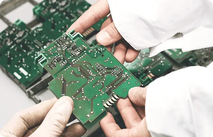
The short version: a single-sided board is not cheap because the process was trimmed. It is cheap because of the material and the one copper layer together, and that same pair hands you every limit you will hit. One copper layer means four things have no fallback: crossings, heat, mechanical strength, and hole metallization. There is no "other layer" to take any of them over. What the base material does is redistribute those four limits, deciding which one gets tighter and which one can actually relax. Choosing the wrong material rarely means the board cannot be built. It means the board gets built, and then heat has to be rescued by the enclosure, depaneling has to change method, or the data package comes back from the fabricator with a single question: which route is this board supposed to run.
1. One copper layer means four things have no fallback
A lot of design freedom on multilayer boards is really the freedom to "solve it on another layer." A single-sided board does not have that option, so four things become hard constraints:
- Crossings. Two nets that need to cross have no second layer to borrow. You route around it, you use a jumper, or you change the circuit topology.
- Heat. Heat can only spread laterally in that one copper layer and then travel out through the base material. There is no inner copper plane and no plated hole to carry heat to the back side.
- Mechanical strength. Stiffness, bending resistance and tolerance to depaneling stress come almost entirely from the base material. The copper layer contributes little.
- Holes. Holes on a single-sided board are usually not plated, so they do not carry layer-to-layer connection. They carry mounting, location, and lead pass-through.
These four are not a list of shortcomings; they are boundary conditions. Treat them as shortcomings and you will spend the project trying to claw each one back. Treat them as boundaries and the design lands in the right place from the start. How fine a trace is actually buildable on a single-sided board is a separate manufacturability review; this article works one level up, on how those constraints get redistributed by the material.
2. Four material families, four different things traded away
Single-sided boards run on four material families in practice. They are not a quality ranking. They are four different places for the cost to land.
1. FR4 (woven glass / epoxy)
The general-purpose choice. Its defining property is that nothing about it is the weakest link: dimensional stability, thermal endurance, mechanical strength and insulation all sit inside a usable range, so it rarely becomes the root of a problem.
- What it trades away: the lowest cost tier. It costs more than paper-based laminate.
- What it buys: process latitude. Reflow, wave, rework and downstream machining all behave predictably.
- Depaneling: routing and V-cut both work. Punching does not — woven glass wears punch tooling and the cut edge quality is not stable.
2. CEM family (composite laminates)
Composite constructions combining glass with paper or non-woven layers, positioned between FR4 and paper phenolic.
- What it trades away: part of FR4's mechanical and thermal margin.
- What it buys: an intermediate cost point, plus some machining behaviour that is friendlier than pure woven glass.
- Watch out: CEM is a family, not one material. The spread between constructions can exceed the gap between "CEM and FR4." Writing only "CEM" in the data package is therefore not enough — either name the grade or state the properties you actually require.
3. Paper phenolic (paper-based laminate)
The traditional low-cost route, common in appliances, lighting and simple control products.
- What it trades away: thermal margin, dimensional and insulation stability after moisture uptake, and tolerance for repeated rework.
- What it buys: the lowest material cost, and crucially punchability. In volume, punching is far faster than routing, and that is often where the real cost advantage comes from, not from the laminate price itself.
- Watch out: it behaves differently under heat than FR4 and the soldering window is narrower. Process and rework have to be planned around its properties, not copied from FR4 practice.
4. Metal core (aluminium, single conductive layer)
Swap the base material for metal. The conductive layer is still one layer, but the thermal path is rewritten entirely.
- What it trades away: cost (above FR4) and some freedom in machining and depaneling — metal-backed boards are profiled and separated by a different set of processes.
- What it buys: heat leaves the copper, passes through the dielectric into the metal base, and exits through the structure. The hardest problem of a single copper layer is carried by the material itself.
- Watch out: the dielectric layer is simultaneously the thermal and the dielectric-strength bottleneck, and those two constrain each other — covered separately. Aluminium machining boundaries are also discussed on their own.
General material selection criteria across any layer count are in the base material article. This piece only looks at how these four differ under the single-sided condition.
3. A jumper is not a design flaw, it is a formal structure
Once you commit to single-sided, jumpers stop being a workaround and become a structure that has to be formally designed and declared. There are two kinds, and they belong to different owners:
- Component-side jumpers (zero-ohm resistors, jumper parts, lead wires): assembly scope. They need a footprint, a reference designator, a BOM line, and an orientation requirement if one applies. The assembly process has to know they exist. This is not the fabricator's business.
- Board-side handling (widening a detour, changing topology, pushing a crossing under a component body): routing scope, owned by design.
What matters is not letting the two blur together in the data package. The classic failure: the schematic shows a jumper, but it has no footprint and no designator, so the BOM is short a line and nobody finds out until assembly. Or the inverse — jumper pads exist on the board but their purpose is never declared, so the fabricator treats them as ordinary pads and the surface finish and mask opening may not suit.
When the jumper count passes a certain point, there is a question worth asking out loud: keep stacking jumpers, or move to double-sided. That is a cost comparison, not an engineering preference. Whatever the single-sided material and process saved has to be weighed against jumper part cost, the assembly step, and the defect risk that one more manual operation introduces. The plated-through-hole process on double-sided boards is described separately and makes a reasonable basis for that comparison.
4. Heat and current: one copper layer can only spread sideways
There is no inner plane and no plated hole to move heat to the back side. So heat has exactly two routes: spread laterally in the one copper layer, and pass through the base material to the outside.
That settles several things:
- Copper area becomes the primary tool. Dissipating parts need continuous copper around them for spreading, not just a pad. How copper area shapes heat distribution is covered on its own.
- Current capacity comes from width and thickness only. There is no "parallel it across layers" option here. Copper thickness options and the design rules that follow are in the copper thickness article. Note that raising copper thickness tightens etch undercut and minimum width/spacing at the same time — one decision, two consequences.
- The base material decides how open the "through" route is. Neither paper-based laminate nor FR4 is a good conductor in that direction. Making that route real usually means moving to a metal core, or accepting that the enclosure, heatsink or potting carries the primary thermal path. Base-metal differences are covered in the metal core article.
One judgement call belongs here: if the thermal requirement has to be met by the board itself rather than by surrounding structure, staying on a non-metal single-sided board is usually not the right answer. That is not a process capability question. It is a question of where the thermal path physically goes, and process cannot claw it back.
5. Strength and depaneling: punch or route is decided by the material
Depaneling method often drives cost directly, and which methods are available is decided by the material, not picked from a menu:
- Punching: highest throughput in volume, but the material has to suit punching and a die has to be made. Paper-based laminates are the typical fit; woven-glass constructions normally do not take this route.
- Routing (profiling): general purpose, good edge quality, widest applicability, higher per-piece time than punching.
- V-cut: suits straight-line separation of regular rectangular arrays, and requires the board shape and layout to cooperate.
Outline tolerances and the related process constraints are in the profiling and V-cut article; array layout constraints are in the panelization article.
The part that gets missed: the depaneling method constrains the board edge design in return. A punched edge, a router bit radius and a V-cut remaining web each place different requirements on what can and cannot sit near the edge. Component, trace and opening clearances to the edge should follow the actual depaneling method, rather than being drawn first and separated later. Dimensional and tolerance conventions are on the tolerance page.
And one property belongs purely to the material: a single-sided board's bending resistance is essentially all base material. Heavy components, connector insertion force, screw clamping during assembly — those loads are carried by the laminate. Paper-based grades have visibly less margin here than FR4.
6. Unplated holes change what a hole is for
Holes on a single-sided board are usually left unplated. That is not "one process step skipped" — the function of the hole is different:
- It no longer provides layer-to-layer connection, so there is no barrel copper reliability concern and no barrel-to-pad interface concern.
- It mainly carries mounting, location and through-hole lead pass-through. The requirement shifts from electrical continuity to positional and dimensional fit.
- A through-hole solder joint forms only on the side that has copper. The relationship between component side and solder side has to be explicit in the data package; the fabricator should not have to guess which face carries copper.
This is where single-sided data packages fail most often: which face is the copper face must be stated explicitly. Legend, solder mask, surface finish and component outline each need a declared side. On a multilayer board that information falls out of the stackup; on a single-sided board there is no stackup to fall out of, so it only exists if you note it.
7. Surface finish and material recognition: two declarations that get skipped
Surface finish is still a real choice on a single-sided board rather than a default. It affects solderability shelf life, storage requirements and the assembly window. Scope and differences between finishes are in the surface finish comparison. The common mistake is to leave it out of the data package entirely and let the fabricator take the cheapest option — which may not suit a product with a storage period or multiple thermal excursions.
Material recognition (UL and similar) is a design input, not a certificate added afterwards. If the end product's compliance route requires the laminate to hold a particular recognition, the material shortlist is already narrowed during design and cannot be swapped after prototyping — a swap means re-verification. How material recognition feeds structural design inputs is covered separately. The materials available at SKPCB are listed on the materials page, and the overall manufacturing envelope on the capabilities page.
8. What the drawing must state before the lowest-cost route can be released
Single-sided data packages are often thinner than multilayer ones, and that is exactly why they generate questions. For a fabricator to release the job, at minimum these have to be unambiguous:
- Material family or grade. "FR4" alone is fine in many cases, but thermal, flammability, CTI or recognition requirements push it to a named grade or an explicit property requirement. "CEM" alone is usually not enough.
- Which face carries copper, and which face carries mask, legend and surface finish.
- Copper thickness, and which trace widths are functional requirements that the fabricator may not adjust within its process.
- Depaneling method (punch / route / V-cut) and the matching edge requirements. Punching also implies tooling, which is a separate engineering decision.
- Which dimensions are fit dimensions — mounting holes, connector positions, critical outline edges. Those need tolerances; the rest can follow standard practice.
- Jumper ownership: which are assembly parts (BOM lines) and which are only routing detours.
- Thermal intent: if a copper area exists as a spreader, say so. Otherwise it reads as an empty pour.
Of the seven, items 1, 2 and 4 go missing most often, and all three are the kind the fabricator cannot decide alone. Guessing wrong costs either a query that stalls the job, or a board built to someone else's interpretation.
9. Decision order: heat and depaneling first, cost last
Putting the sections together, a reasonably robust order for single-sided selection:
- Does the thermal requirement have to be met by the board? If yes, go to metal core directly, do not look for workarounds on a non-metal laminate. If no, continue.
- Is punching required? If yes, the material shortlist narrows to punchable grades and die cost enters the comparison. If no, routing or V-cut leaves far more material freedom.
- Are there thermal, humidity, recognition or repeated-rework requirements? If yes, paper-based margin is usually insufficient; move toward FR4/CEM.
- Are mechanical loads significant (heavy parts, insertion force, screw clamping)? If yes, favour FR4.
- Has the jumper count gotten out of hand? If yes, recompute total cost for "single-sided plus jumpers" against double-sided. Do not settle this one by preference.
- Only once the above hold, take the cheapest remaining material.
The point of that order: cost sits last not because it does not matter, but because the first five all contain something process cannot recover. Fix cost first and trim requirements backwards, and the problem usually surfaces after prototyping. The single-sided product scope is on the single-sided page, the crossover case on the double-sided page, the thermal route on the aluminium page, and inspection and release conventions on the quality page. The fine-line process boundary itself is in the fine-line manufacturing article.
FAQ
Q: How complex a circuit can a single-sided board carry?
A: There is no useful general ceiling beyond layer count itself; the real limit is the number of crossings. The more nets that must cross, the longer the detours get and the more fragmented the copper becomes, or the more jumpers you add. Once the jumper count starts dictating how assembly is organised, the complexity has left the economic range of single-sided — and at that point the deciding factor is total cost, not whether single-sided "can" do it.
Q: How far apart are paper phenolic and FR4, and when is FR4 mandatory?
A: What manufacturing can speak to is the nature of the difference rather than a numeric ranking: paper-based grades have less thermal margin, less dimensional and insulation stability after moisture uptake, and less tolerance for repeated rework than FR4; in exchange they are punchable and cost less. FR4 or CEM is normally the answer when any of these apply: a demanding thermal or humidity requirement, mechanical load in assembly (heavy parts, insertion, screw clamping), the need for repeated rework, or a compliance route requiring a specific material recognition. For simple, low-load volume parts on a punching route, paper-based is often the right fit.
Q: Can heavier copper solve heat on a single-sided board?
A: Only part of it, and only the lateral spreading part. Heat still has to pass through the base material to leave, and neither paper-based laminate nor FR4 is a good conductor in that direction. Heavier copper also tightens etch undercut and minimum width/spacing, so it is not free. If the board itself must carry the thermal duty, a metal core is usually the correct answer; if surrounding structure can carry it, assign that responsibility to the mechanical design explicitly instead of expecting copper thickness to cover it.
Q: Do jumpers belong in the BOM?
A: Component-side jumpers (zero-ohm resistors, jumper parts, lead wires) do — they need footprints and designators because they are assembly parts. Pure routing detours involve no material and do not. The two must be separated in the data package; the most common incident is a schematic jumper with no designator and no footprint, discovered as a missing BOM line during assembly.
Q: How do I choose between punching and routing?
A: Check the material first. Paper-based grades suit punching; woven-glass constructions normally do not take that route. Where punching is allowed, run the volume: a die has to be amortised, so it pays off only above a certain quantity. If volume is modest or the outline may still change, routing is safer. V-cut applies to straight-line separation of regular rectangular arrays. Once chosen, go back and check the board edge design matches the method, not the other way around.
Q: Should single-sided holes be plated?
A: Normally not. They carry mounting, location and lead pass-through rather than layer-to-layer connection, so the requirement is positional and dimensional fit rather than barrel copper reliability. If the circuit genuinely needs a hole to connect two faces, the real requirement has already become a double-sided board.
Q: What is most often missing from a single-sided drawing?
A: Three items: material family or grade (naming only "FR4" or "CEM" is not enough when thermal, flammability or recognition requirements exist), which face carries copper (along with the sides for mask, legend and finish), and depaneling method with its matching edge requirements. All three are things the fabricator cannot decide alone, so the result of omitting them is either a stalling query or a board built to someone else's reading.
---