


1. "Aluminum PCB, 1.6 mm" on a drawing still leaves the shop guessing
The most common line in an aluminum PCB enquiry is "Aluminum PCB, 1.6 mm, 1oz copper". It looks complete — thickness and copper weight are both there — yet the one layer the shop actually needs confirmed is missing: the thermally conductive dielectric between the aluminum base and the copper foil.
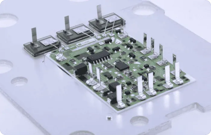
An aluminum PCB is not a sheet of aluminum with traces printed on it. Per the construction described on our Aluminum PCB page and Metal Core PCB page, it is three layers: metal base, thermally conductive dielectric, copper circuit layer. Only one of those three carries two directly conflicting jobs — conduct heat downward while blocking voltage upward. Leave it off the drawing and both the thermal target and the insulation requirement are handed over as guesswork.
So this article is not "what is an aluminum PCB". Structure, base-metal selection and the thermal-via comparison are already covered in our Aluminum & Metal-Core PCB Thermal Management guide. This one answers a single specification question: on the same drawing, how do you write the conductivity requirement and the withstand-voltage requirement so that both hold?
> Division of roles: the Aluminum PCB product page owns the board-type overview and the engineering-review entry point — it answers "what range can be built". This article answers "how do I write the requirement, and what is left once I have". Each links to the other.
2. The bottleneck is the dielectric, not the metal
Start with the magnitudes. The conductivity figures already published in our thermal management guide:
| Material | Thermal conductivity (approx.) |
|---|---|
| Copper | ≈385 W/m·K |
| Aluminum | ≈205 W/m·K |
| Dielectric, standard epoxy / ceramic-filled | ≈1–3 W/m·K |
| Dielectric, high performance | ≈5–8 W/m·K |
| FR-4 glass-fibre substrate | ≈0.3 W/m·K |
Nearly two orders of magnitude separate the metal from the dielectric. Put plainly: along the path from component pad to metal base, most of the temperature drop sits in that one thin dielectric layer. Swapping aluminum for copper (≈205 → ≈385) improves lateral spreading, but if the dielectric stays in the low band, the dominant term in the overall thermal resistance has not moved.
That is why the dielectric should be specified first and the base metal second. Choosing base thickness first and remembering the dielectric last usually produces a board with plenty of aluminum and nowhere for the heat to go.
3. 1.0–3.0 vs 1.0–8.0: two ranges, two product pages, no mixing
This is where real drawings go wrong most often. The two board-type pages publish different conductivity ranges:
| Specification | Aluminum PCB (/products/aluminum-pcb/) | Metal Core PCB (/products/metal-core-pcb/) |
|---|---|---|
| Base material | Aluminum alloy base | Aluminum / copper base |
| Thermal conductivity | 1.0–3.0 W/m·K | 1.0–8.0 W/m·K |
| Metal base thickness | 0.8–3.0 mm | 0.8–3.0 mm |
| Copper thickness | 1oz–6oz | 1oz–10oz |
| Layers | 1–4 layers | Single / double sided |
| Max board size | 1500×600 mm | 1200×600 mm |
| Surface finish | HASL / ENIG / OSP | HASL / ENIG / OSP |
| Dielectric withstand voltage | ≥3000V | — |
State which page you are quoting. A drawing that says "dielectric conductivity 6 W/m·K, per the aluminum PCB page" will come back for clarification — that value belongs to the metal core range, not to the 1.0–3.0 published for aluminum. Equally, lifting the ≥3000V figure from the aluminum page onto a copper-base construction needs review, not copy-paste.
The two pages cover different board types and different specification sources, so cross-references must be resolved item by item rather than merged into one "general" table. The same applies to panel size: the 1250×570 mm on our Capabilities page is the site-wide process figure, and aluminum 1500×600 and metal core 1200×600 are two further independent figures. Cite them per board type.
4. The voltage side: a thinner dielectric lowers thermal resistance and cuts voltage margin
The Aluminum PCB page publishes a dielectric withstand voltage of ≥3000V. That gives specification writing a floor, but it is not a guarantee that holds under any construction — it is coupled to the dielectric formulation band, its thickness, the copper weight and the board layout.
The trade-off is direct:
- Thinner dielectric → lower thermal resistance (better heat transfer) → but a thinner insulator, so less voltage margin and tighter long-term insulation reliability.
- Thicker dielectric → more voltage margin → but higher thermal resistance, and the thermal target may not be met.
- Higher filler loading → conductivity rises → but the mechanical and insulation behaviour of the material changes and needs re-review.
"Highest conductivity, highest withstand voltage, thinnest dielectric" therefore cannot all be satisfied at once. The drawing has to declare which one is the hard requirement: hold the insulation class and optimise conductivity underneath it, or fix the thermal target and then confirm whether the voltage requirement is still met. A specification that does not declare this will come back at engineering review.
Actual dielectric thickness, thermal resistance values and withstand-voltage test conditions are project parameters confirmed by engineering review against the real construction; this article publishes no generic numbers for them.
5. What is left once the dielectric is fixed
The dielectric line does not stand alone. Fixing it pins down several other items at the same time:
- Copper weight: the aluminum page publishes 1oz–6oz. Higher copper for lateral spreading or current capacity moves you into the 1oz–10oz range of the metal core page, which changes the board-type basis.
- Layer count: the aluminum page publishes 1–4 layers. Dielectric parameters and layer count are reviewed together, not layer count first and dielectric squeezed in after.
- Panel size: aluminum 1500×600 mm, metal core 1200×600 mm. Panelisation and the separation method (the aluminum page publishes V-cut scoring as available) must be confirmed together with the dielectric, because depanelisation stress acts on the dielectric-to-copper bond.
- Surface finish: HASL / ENIG / OSP, chosen alongside the assembly thermal history — see our Surface Finish page.
- Thickness tolerance: per our Manufacturing Tolerance page, finished thickness is judged as "±10% or ±0.005", whichever is greater" (that page states imperial values are authoritative, per IPC-6012, 1 inch = 25.4 mm). Dielectric thickness is part of the finished stack, so the tolerance cannot be tightened in isolation.
6. When to leave aluminum behind
An aluminum PCB is not the answer to every thermal problem. Two clear forks:
- When power density or operating temperature approaches the limit of an organic dielectric, evaluate ceramic. Per our Ceramic PCB page, the specification range is 24–230 W/m·K, 0.25–2.0 mm thickness and −55 °C~850 °C temperature resistance, with an inorganic dielectric that has no organic thermal-ageing path. Our Ceramic Substrate PCB guide covers the selection logic.
- When the real constraint is current, not heat, the direction is heavy copper, not aluminum. Per our Heavy Copper PCB page, the range is 3oz–>12oz copper, 1–16 layers, 0.8–6.0 mm board thickness and 6 mil minimum trace width. That solves current with copper cross-section, a different route from solving heat flow with a metal base.
Recommended order: confirm whether the limit is thermal or electrical, then choose the board type, then write the dielectric or copper specification. Doing it backwards usually means rework.
7. The lines that actually belong on the drawing
Collapsing the above into a list you can copy. An aluminum PCB drawing or specification should state at minimum:
- Board type and source page: aluminum PCB (per
/products/aluminum-pcb/) or metal core PCB (per/products/metal-core-pcb/), naming which specification range you are citing. - Dielectric conductivity requirement: as a range rather than a single point, and marked as either a hard requirement or a target.
- Withstand-voltage requirement: the class to be met; the ≥3000V published on the aluminum page can serve as the cited floor. Test conditions and acceptance method are confirmed in the project documents.
- Metal base thickness: a nominal value within 0.8–3.0 mm.
- Copper weight: within 1oz–6oz (aluminum) or 1oz–10oz (metal core).
- Surface finish: one of HASL / ENIG / OSP, with the assembly process stated.
- Which item is a critical dimension or critical characteristic: mark it explicitly to avoid repeated review cycles.
- Finished thickness tolerance form: cite the
/tolerance/basis, or state your own and define what is measured.
With those eight lines the engineering review can go straight to feasibility instead of returning a "please confirm the dielectric" query first. To have the feasible window confirmed against your real construction, submit Gerber data, stack-up intent and the thermal / insulation targets through our quote and engineering review entry; acceptance basis is described on the Quality Assurance page.