


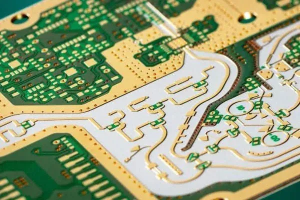
High frequency boards rarely fail because the fab cannot build them. They fail because the drawing did not say. Many FR-4 defaults do not hold on an RF board: the dielectric, copper foil, surface finish or solder mask coverage a fab picks by habit can shift insertion loss, impedance or phase matching.
Fabrication notes replace those defaults with stated requirements. The eight items below follow the order of a fab's engineering review, and each one notes what usually happens when it is missing.
1. Material: part number, thickness and substitution rule
"Rogers laminate" is not enough. Give the exact material, core thickness and copper weight, and state whether substitution is allowed and who approves it.
If this is missing, the fab picks from stock or its usual grade, or raises an engineering query and waits. Hybrid boards (RF cores plus FR-4) must also state which layers use the RF material.
SKPCB works with Rogers 4350B/4003C/3003, Arlon 85N and Taconic RF-35; see High Frequency PCB. Criteria for approving a substitute are covered in High Frequency Laminate Substitution Approval.
2. Stackup: dielectric thickness and layer order
Impedance and loss on an RF line depend directly on the dielectric between signal and reference layer. The stackup drawing should show every copper layer, every dielectric (core or prepreg) with part number and target thickness, and where the RF layers sit.
If this is missing, the fab works backward from the impedance target. The result may hit impedance while the dielectric thickness no longer matches your simulation model, so loss and phase drift.
3. Impedance: target, tolerance and test method
List each controlled line: layer, reference layer, width and spacing, target impedance and tolerance. State whether testing uses a coupon or on-board traces, and whether a report is required.
SKPCB's standard impedance tolerance is ±10%; ±5% requires engineering review. See Impedance Control PCB. Coupon design and verification are covered in Impedance Test Coupon Verification.
If this is missing, the fab applies a general tolerance and its own test method, and the data you need may not ship with the boards.
4. Copper foil type
At high frequency, conductor loss depends on copper surface roughness. If the simulation assumes low-profile foil, the notes must name the foil type or state "manufacturer's standard foil for this laminate, no change permitted."
If this is missing, the fab may use another foil option for the same laminate. The mechanism is explained in High Frequency Copper Foil Roughness and Insertion Loss.
5. Surface finish and zoning
The surface finish sits in the RF current path. State the finish type and, on mixed boards, whether the RF and digital zones differ and where the boundary is.
If this is missing, the fab applies one finish to the whole board. Process constraints by finish are compared in PCB Surface Finish Comparison.
6. Solder mask coverage
Solder mask over a microstrip changes effective dielectric constant and loss. The notes must say whether RF lines are mask-free, where the opening boundary is, and whether the simulation includes the mask.
If this is missing, the fab normally covers the whole board, and the actual impedance and loss of RF lines may not match simulation.
7. Drilling and hole metallization
Hole wall preparation in PTFE-type materials differs from FR-4. State hole sizes and plating requirements, via fence and ground via locations, and any backdrill, plugged or blind vias.
If this is missing, the fab builds to general plating requirements and default structures, and RF transition parasitics are hard to align with the design.
8. Acceptance class and reports
State the acceptance basis (for example IPC-6012 Class II or Class III, or IPC-6018 for high frequency boards) and the reports to ship with the order: impedance test report, microsection report, material certificate.
SKPCB accepts to IPC-6012 Class II and Class III; see Quality Assurance.
If this is missing, the fab accepts to its default class and ships only standard reports.
Pre-release check order
- Material part number, thickness and substitution rule stated;
- Stackup drawing lists every dielectric with part number and thickness;
- Impedance table gives layer, reference, width, target and tolerance, plus test method;
- Copper foil type stated or locked;
- Surface finish and solder mask zones marked on layers or drawing;
- Hole structures and plating requirements stated;
- Acceptance class and report list given.
When the package is complete, submit it through the quote page; engineering review confirms each item.
Summary
High frequency PCB fabrication notes should turn eight items into checkable requirements: material, stackup, impedance, copper foil, surface finish, solder mask, holes and acceptance. Any blank gets filled with standard-board practice, which may not suit an RF design.
FAQ
Q: Is "Rogers 4350B" enough on the drawing?
A: No. Add core thickness, copper weight, foil type and whether substitution is allowed.
Q: Should impedance be tested on a coupon or on board traces?
A: Either works, but specify which. Coupons are easier to measure; on-board traces are closer to the real routing.
Q: Should RF lines have solder mask?
A: It depends on the simulation model. If the model excludes mask, open the mask over RF lines and mark the boundary.
Q: What extra information does a hybrid board need?
A: Which layers use RF material, which use FR-4, and the dielectric thickness of each.
Q: What standard applies to high frequency board acceptance?
A: IPC-6012 Class II or Class III is common; IPC-6018 can also be referenced. Specify it in the notes.
Q: What happens if these requirements are left out?
A: The fab raises engineering queries or fills gaps with standard-board practice, which can push impedance and loss away from simulation.