


Mask or air above the trace is itself a design parameter
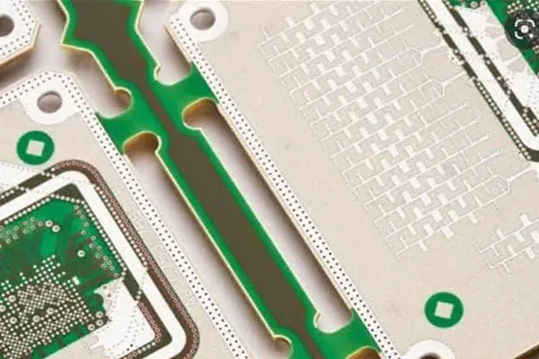
The impedance and loss of an outer-layer microstrip depend on the dielectric below the trace and on whatever sits above it. On a typical digital board, solder mask is a protection layer. On a high frequency board, it is an extra dielectric layer with its own properties and thickness variation, sitting directly on the RF conductor.
So the solder mask question on an RF board is not "green or not". It is three linked decisions:
- whether RF traces and structures are covered by mask or left open;
- which surface finish protects the copper once it is exposed;
- whether the laminate allows the mask to adhere reliably and register accurately.
Diagram suggestion: two microstrip cross-sections side by side, left "trace with mask cover", right "trace opened with surface finish". Mask in teal, laminate in deep blue, arrows showing the field passing through mask versus air.
Covering vs opening: what each buys and what each costs
| Choice | What it buys | What it costs |
|---|---|---|
| Mask over RF traces | Copper protected from oxidation, scratches and solder bridging | Mask becomes the dielectric above the trace; its thickness and property variation enter impedance and loss |
| RF traces opened | Simpler, more predictable dielectric environment above the trace | Bare copper needs a surface finish, which itself enters conductor loss; edge and mechanical protection is weaker |
| Partial opening (RF area only) | Predictable RF area with protection elsewhere | Registration of the opening boundary and mask dams become new process control points |
No single choice is right for every design. The deciding factors are which state the simulation model assumes, whether the RF area will be touched during assembly and use, and whether the surface finish stays within acceptable loss.
Areas that usually need an opening discussion first
- RF microstrip and coplanar waveguide: if the impedance model assumes no mask, covering the trace moves it away from the model.
- Couplers, filters and other distributed structures: their geometry is sensitive to the surrounding dielectric, so mask coverage changes the response.
- Antenna radiators: the dielectric above affects radiation behaviour and must be agreed with the antenna designer.
- Ground copper and via fences in grounded coplanar structures: often opened together with the RF trace to keep the structure consistent.
- Connector and RF component pads: these are opened anyway, but the distance from the opening edge to the trace needs to be defined.
Digital, power and control areas normally keep standard mask coverage.
After opening: surface finish and mask are decided together
Once an RF area is opened, the surface finish protects the copper and becomes part of the RF conductor. The linked points:
- Nickel-containing finishes: the nickel layer sits at the conductor surface, where high frequency current concentrates, so its effect on conductor loss needs to be assessed during selection.
- Nickel-free finishes: immersion silver, OSP or immersion tin are often considered for loss reasons, but each has its own storage, handling and solderability window.
- Selective finishes: when the RF area and the rest of the board use different finishes, the boundary between mask and plating resist and the process sequence must be confirmed before fabrication.
A general comparison is in PCB surface finish comparison; the finishes SKPCB offers are listed on the surface finish page.
Process constraints of solder mask on RF laminates
Mask process experience from FR-4 does not transfer directly to RF laminates:
- Adhesion: some RF laminates, PTFE-based ones in particular, have low surface energy and need dedicated surface preparation before mask. Insufficient preparation can lead to lifting or peeling.
- Effect of pre-treatment on copper: roughening copper to improve mask adhesion changes the copper surface, which conflicts with the goal of choosing low-profile foil. The trade-off has to be made deliberately. See copper foil roughness and insertion loss.
- Registration and opening edges: the closer the opening edge is to an RF trace, the more mask registration variation affects the local trace environment. The edge position should be defined by the design.
- Mask thickness uniformity: with a covered design, mask thickness on top of the trace, at its sides and between traces is inherently uneven, and this shows up in impedance test results.
- Impedance test conditions: coupons measured before and after mask give different results. The coupon mask state should match the RF area of the product.
Overall process control for RF boards is covered in high frequency PCB fabrication process control.
What the drawing and fabrication notes should state
- Mask state in RF areas: covered, opened or partially opened, with the area defined on a dedicated mask layer or note.
- Opening boundary: the edge of the opening relative to RF traces and structures is set by the design, not left to default fab expansion rules.
- Simulation basis: which mask state the impedance and loss model assumes, with test coupons built in the same state.
- Surface finish: whether RF and non-RF areas share the same finish, and if not, how the zones are split.
- Mask material requirements: whether a mask type is specified or restricted; without this the fab uses its standard material.
- Cosmetic and protection criteria: how scratches and oxidation in opened areas are judged at inspection.
Without this information, the fab can only apply digital-board habits to the mask, and the result often differs from the RF simulation model. See the high frequency PCB page for fabrication scope, and attach these notes when using the quote page.
FAQ
Q: Do RF traces on a high frequency PCB always need a mask opening?
A: Not always. An opening makes the dielectric above the trace more predictable, but the bare copper then needs a surface finish that carries its own loss effect. The decision depends on the simulation model, assembly protection needs and finish selection together.
Q: Can the effect of mask over an RF trace be ignored?
A: It should not be ignored by default. Mask is a dielectric layer above the trace, and its property and thickness variation feed into impedance and loss. How much it matters depends on the frequency range and structure, so model the actual state in simulation.
Q: Which surface finish suits opened RF areas?
A: There is no universal answer. Nickel-containing finishes need their nickel effect on conductor loss assessed; nickel-free finishes are often preferred for loss but have storage and solderability constraints. Choose together with RF requirements and the assembly process.
Q: What tends to go wrong with solder mask on PTFE laminates?
A: Mainly adhesion. These materials have low surface energy and need dedicated surface preparation; without it, mask can lift or peel.
Q: Should impedance coupons carry solder mask?
A: The coupon mask state should match the product RF area. If the RF area is opened, open the coupon; if it is covered, cover the coupon. Otherwise the measurement does not represent the product.
Q: Is "green solder mask" on the drawing enough?
A: No. State at least the RF mask state, opening boundaries, finish zoning and simulation basis, otherwise the fab will follow digital-board defaults.