


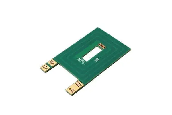
Many heavy copper drawings state a single copper weight, such as "outer layers 6 oz", and then pick a trace width from a current chart. The chart assumes an ideal rectangular cross-section. The conductor that leaves the factory is not rectangular. What actually sets temperature rise is the finished cross-section at the narrowest point, together with how well that conductor can shed heat.
Copper weight is a mass-per-area unit. By industry convention, 1 oz/ft² corresponds to roughly 35 µm of copper, but that is only the starting point. Between the nominal weight and the finished cross-section sit four things: how the copper thickness is built up, what shape etching leaves behind, which side of the width tolerance the trace lands on, and where the narrowest section of the current path is.
Nominal copper weight is not finished thickness
Outer-layer conductors are normally base copper plus plated copper. Inner-layer conductors are usually base copper only. Two layers both labelled "3 oz" can therefore finish at different thicknesses. If the drawing does not say whether the weight means base or finished copper, the fabricator has to fall back on convention.
Heavy copper also loses some thickness during processing: micro-etching before surface finish and mechanical brushing both remove copper. The thicker the copper, the smaller this loss is in relative terms, but it does not disappear.
Design input: state whether the weight is base or finished, separately for inner and outer layers. If you need a guaranteed minimum, specify a minimum finished copper thickness rather than a nominal oz value.
Etching turns the cross-section into a trapezoid
Etching works downward from the copper surface, and the thicker the copper, the more pronounced the side etch. A heavy copper conductor therefore usually has a trapezoidal cross-section: the bottom is close to the design width, the top is narrower. Its area is smaller than the simple width × thickness estimate.
Fabricators apply etch compensation to heavy copper, widening the artwork so the finished bottom width returns to the design value. Compensation restores width; it does not remove the trapezoid. The method is covered in heavy copper etch compensation review.
Design input: size current-carrying conductors on a trapezoidal section with margin, not on a rectangular section at the limit. Agree with the fabricator whether width is measured at the top or the bottom.
Which side of the width tolerance you land on
SKPCB's trace width tolerance is ±20%. On a signal line this affects impedance. On a power conductor, a negative deviation removes cross-section directly. A trace sized to be "just enough" on a current chart will run hotter if it finishes at the low end.
Design input: choose power trace widths so they still meet the requirement after negative tolerance. Critical conductors can carry a separate minimum finished width on the drawing.
Inner and outer layers dissipate heat differently
The same cross-section heats up differently on an outer layer and an inner layer. An outer conductor can release heat to air; an inner conductor is surrounded by dielectric and can only conduct heat through the laminate and neighbouring copper. IPC-2152 treats internal and external conductors, board thickness and nearby copper planes as separate conditions for exactly this reason.
So the layer a power path runs on is part of the current design. An internal high-current path often needs a larger section, or adjacent copper planes to help pull heat away. Stackups that combine weights are covered in heavy copper multilayer mixed-weight stackup.
Design input: give the conductor layer, any adjacent large copper areas, board thickness and ambient conditions together with the current requirement.
The bottleneck is often not the conductor itself
A wide, thick copper bar still has to bring current on and off the board through pads, vias or connector pins. Those features usually have a far smaller cross-section than the conductor:
- Necking: a conductor narrowed locally to pass a hole or component. The narrowest point sets the temperature rise of that segment.
- Vias and via arrays: when current changes layers, it flows only through the plated barrel. Barrel copper is much thinner than a heavy copper layer, so enough vias must share the current. Plating acceptance criteria are covered in PCB electroplating quality inspection and release.
- Pads and terminals: current passing from conductor to pad to component or terminal is limited by pad size and the solder joint.
- Thermal relief connections: spoke connections added for easier soldering split the current path into narrow ribs. High-current pads should be evaluated for a solid connection.
Design input: mark every layer transition and every narrowest point on the current path. At transitions, state via count and hole size; on high-current pads, state the connection style.
How to write a current requirement
"This board carries high current" is not a reviewable input. A current specification that both designer and fabricator can work from includes at least:
- Continuous and peak current for each high-current path, and peak duration;
- Allowed temperature rise or maximum conductor temperature;
- Conductor layer, board thickness, adjacent copper and cooling conditions (airflow, heatsink, enclosure);
- Copper weight definition (base or finished) and minimum finished thickness;
- Minimum finished width of critical conductors, plus via count and hole size at layer transitions.
How to choose a copper weight tier is discussed separately in heavy copper 3 oz vs 6 oz vs 12 oz+ copper weight tiers. SKPCB's maximum copper thickness is above 12 oz; see heavy copper PCB for product capability. Specific weight and width combinations require engineering review.
How to verify the finished cross-section
A cross-section cannot be judged by eye. Release depends on measurement:
- Microsection: cut a coupon or a specified location and measure finished copper thickness, top width and bottom width to confirm the section shape.
- Width measurement: measure finished width on critical conductors and confirm it is within tolerance and above any stated minimum.
- Barrel copper: measure via wall copper thickness on the microsection.
- Loaded temperature-rise test: test a prototype at real current and cooling conditions. This is the most direct check of a current design and is usually performed by the designer on the product or a test fixture.
If you need a microsection report or specific measurement locations, state them in the order package and submit them through the quote page.
Summary
Heavy copper current capacity is set by the finished cross-section at its narrowest point and by the cooling conditions, not by nominal copper weight. Size conductors on a trapezoidal section with negative tolerance, include layer position, transition vias and pad connections in the calculation, write the requirement as measurable inputs, and verify with microsections and temperature-rise testing.
FAQ
Q: How much current can a 4 oz copper trace carry?
A: There is no single number. It depends on finished cross-section, layer, allowed temperature rise and cooling. Calculate it with the IPC-2152 method for the actual conditions and confirm with a prototype temperature-rise test.
Q: Why do inner-layer conductors need to be wider at the same copper weight?
A: Inner conductors are surrounded by dielectric and dissipate heat less effectively. For the same current and temperature rise, they usually need a larger section.
Q: Does etch compensation remove the trapezoidal profile?
A: No. It brings the finished bottom width close to design, but the heavy copper section stays trapezoidal and its area is below the rectangular estimate.
Q: Should the drawing state base or finished copper weight?
A: Both conventions exist; what matters is stating which one. When cross-section must be guaranteed, a minimum finished thickness is more reliable.
Q: How many vias are needed for a high-current layer change?
A: It depends on current, hole size and barrel copper. Barrel copper is much thinner than a heavy copper layer, so transitions usually need several vias in parallel; calculate the count and put it on the drawing.
Q: How can I confirm the delivered boards meet the cross-section?
A: Request a microsection report covering finished copper thickness, width and barrel copper. Confirm current capacity itself with a loaded temperature-rise test on prototypes.