


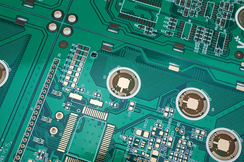
A double-sided PCB is the lowest-cost plated-through-hole construction: two copper layers, one drilling and metallisation sequence, no multilayer lamination. Its problems rarely come from "it won't route." The real limit is that both layers carry traces, so neither layer can act as a continuous reference plane. Return paths, impedance, EMC, power distribution and heat spreading all have to be handled by the routing layers themselves.
Whether to move to 4 layers is not decided by how much routing space the CAD tool has left. It is decided by how many of the following signals show up.
What two layers are actually missing
The most common 4-layer stack-up is signal / ground / power / signal. The two inner layers carry almost no traces; they exist to provide continuous copper. That gives every signal trace a return path directly beneath it and gives the power rails a low-impedance distribution network.
A double-sided board cannot do this. You can flood the bottom layer with ground, but as long as the bottom layer also carries traces, the pour is cut into islands. Return current under a signal trace has to detour around the gaps, and the loop area grows. Almost every electrical problem on a double-sided board traces back to this.
Signal one: return paths under critical nets are cut
Clocks, fast data lines and the high-current loops of switching regulators return along the copper directly under the trace. Once the bottom ground pour is split by routing, that current is forced to detour.
- If a critical net must cross a slot in the bottom pour and cannot be rerouted around it, two layers can no longer carry that group of signals.
- Jumpers or stitching vias across the islands help partly, but every additional crossing is a risk point that needs its own verification.
Signal two: the design calls for controlled impedance
Controlled impedance needs a defined dielectric thickness between the trace and its reference plane. On a double-sided board the reference is on the opposite side, so the dielectric is the full core thickness. That is usually thick, and hitting common impedance targets pushes trace widths to the point where routing becomes difficult.
The alternative is coplanar waveguide (ground copper running alongside the trace on the same layer). It is more sensitive to spacing, pour integrity and solder mask coverage, which makes production consistency harder to hold. Once the design has several controlled-impedance differential pairs or single-ended lines, 4 layers should normally be evaluated. Where impedance deviations come from in fabrication is covered on the impedance control PCB page.
Signal three: thin EMI margin or repeated EMI fixes
Larger loop area means more radiation. The usual EMI fixes on a double-sided board are filtering, shielding cans and slower edge rates. They work, but each one adds material cost or gives up performance.
If the same board has already been through more than one EMI fix cycle, and the root cause is the return path rather than a specific component, moving to 4 layers is often cheaper than adding more external measures, and more likely to pass first time.
Signal four: power distribution relies on wide traces
On a double-sided board power can only be distributed by traces or local pours. With several voltage rails and several high-current loads, power routing competes with signal routing for space, and voltage drop and noise become harder to control.
- A decoupling capacitor is only as effective as the loop inductance between it and the power and ground it serves. Without planes, that loop is made of traces and vias, and its inductance is noticeably higher.
- If signal traces are being pushed into worse positions to make room for power traces, the power distribution is already costing you signal quality.
Signal five: hot components need more copper to spread heat
Heat from power components is often spread through board copper. A double-sided board has only two copper layers, both carrying traces, so continuous spreading copper is limited. On a 4-layer board the inner planes add lateral heat conduction.
If heat is the main problem and electrical complexity is low, heavier copper or a metal-core substrate may solve it without adding layers. The trade-offs are discussed in the multilayer PCB stack-up guide.
Staying at two layers: what you can do and what it costs
Not every signal above forces a layer change. These measures can postpone the decision, each at a price:
| Measure | What it fixes | Cost |
|---|---|---|
| Keep the bottom layer almost entirely ground, route on top | Restores most return paths | Higher top-layer density, may need finer trace/space |
| Stitching vias between the two pours | Lowers impedance between pour islands | More vias, less routing space |
| Coplanar waveguide instead of microstrip | Controlled impedance without inner layers | More sensitive to spacing and pour integrity |
| Filters and shielding cans | Better EMI | Extra material, assembly steps and cost |
| Larger board outline | More room for routing and pours | Not possible when the enclosure is fixed |
Add these costs up together. Quite often the combined material and verification cost of several workarounds approaches, or exceeds, the extra laminate and lamination cost of going to 4 layers.
What changes in fabrication at 4 layers
From the fabrication side, a 4-layer board adds several steps and several inputs that must be frozen before ordering:
- Inner-layer processing and lamination: inner layers are imaged, etched and inspected, then pressed together with prepreg and outer copper foil. A double-sided board has none of this.
- Stack-up and dielectric thickness: on 4 layers, impedance is set by the dielectric between a signal layer and its adjacent plane. That thickness comes from the core and prepreg combination and has to be defined at design stage.
- Symmetry: an asymmetric stack-up or copper distribution raises warpage risk, so inner-layer copper coverage and copper weight should be kept as symmetrical as possible.
- Layer-to-layer registration: through holes must hit pads on every layer, so inner-layer registration affects annular ring.
The 4-layer construction is described on the multilayer PCB page. How to decide further between 4, 6 and 8 layers is covered in multilayer layer count: 4 vs 6 vs 8.
Release inputs: what to freeze for each construction
Before ordering a double-sided board, confirm:
- board thickness, copper weight, surface finish and solder mask colour;
- whether controlled impedance is required (if so, state whether the structure is coplanar waveguide or microstrip and which layer is the reference);
- minimum trace/space, minimum hole size and annular ring;
- component side assignment for double-sided assembly, see second-side reflow on double-sided boards.
Before ordering a 4-layer board, additionally define:
- layer order (which layer is signal, ground, power);
- target board thickness and stack-up requirements, or permission for the factory to propose a stack-up against impedance targets;
- target value, reference layer and routing layer for each impedance-controlled net;
- inner-layer copper weight and any inner-layer high-current requirements.
General file requirements are listed in the Gerber file preparation checklist. With complete data you can request a quote, and the factory will reply with manufacturability comments against your stack-up and impedance requirements.
Summary
The sign that a double-sided board has reached its limit is not that routing space has run out, but that critical nets no longer have a continuous return path. With one signal present, evaluate the two-layer workarounds first. With two or more, or when the workarounds cost about as much as the extra layers, 4 layers is usually the safer choice.
FAQ
Q: Can a double-sided PCB have controlled impedance?
A: Yes, but the reference is either on the opposite side or beside the trace on the same layer, so impedance is set by core thickness or spacing. The adjustable range is narrow and consistency is harder to hold. A few impedance lines are workable; several differential pairs usually justify evaluating 4 layers.
Q: If I flood the bottom layer with ground, isn't that a ground plane?
A: Not while the bottom layer also carries traces. The pour is split and return current has to detour. The fewer bottom-layer traces, the closer it gets to a real plane.
Q: Is 4 layers always much more expensive than 2?
A: 4 layers add inner-layer processing and lamination, so laminate and process cost go up. Compare that against filtering, shielding, EMI rework and board area on the double-sided design; the actual difference needs a design-specific quote.
Q: What is the standard 4-layer layer order?
A: The most common is signal / ground / power / signal. Variants such as signal / ground / ground / signal are used depending on power complexity and return-path needs.
Q: If the only problem is heat, do I need more layers?
A: Not necessarily. With low electrical complexity, heavier copper, more thermal vias or a metal-core substrate may be more direct than adding layers.
Q: What happens if I order without specifying a stack-up?
A: Without impedance requirements, factories usually apply a standard stack-up for the target thickness. With impedance requirements, provide targets and reference layers so the factory can propose and confirm a stack-up.