


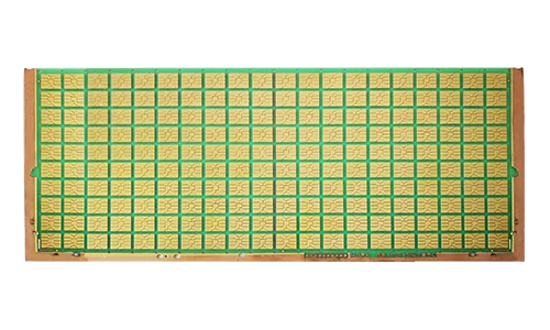
When BGA pitch shrinks, there is no room for dog-bone fan-out between pads, so the via goes into the pad itself. That is via-in-pad. Because the hole sits in a solder land, paste would wick into it during reflow. The hole therefore has to be filled, planarized and plated over, so the pad becomes a continuous, solderable copper surface again. IPC-4761 classifies this structure as Type VII (filled and capped).
SKPCB's plugging capability is described on the resin plugged via PCB page. Acceptance fields and void criteria are covered in resin-filled via acceptance review. This article covers only the process order, the design input behind each step and where failures appear at SMT.
Six steps and their inputs
| Step | Purpose | Designer provides | Symptom at SMT if it goes wrong |
|---|---|---|---|
| 1 Drilling | Form through, buried or laser vias | Hole size, location, which vias sit in pads | Via breaks out of the pad, incomplete land |
| 2 Hole metallization | Plate copper on the hole wall | Hole copper requirement, board thickness | Thin barrel cracks during reflow |
| 3 Resin plugging | Fill the hole with resin | List of vias to plug, plugging type | Voids outgas into solder joint voids |
| 4 Cure and planarize | Cure resin and grind the hole flush | Surface flatness requirement | Dimple or bump, paste volume and coplanarity issues |
| 5 Cap plating | Plate copper over the resin | Whether capping is required, surface finish | Cap separates from barrel, pad lifting |
| 6 Outer layer and solder mask | Form pads and mask | Pad size, mask openings | Pad size deviation, bridging or insufficient solder |
Plugging method: screen printing vs vacuum
SKPCB offers conventional screen-printing and vacuum resin plugging. Screen printing pushes resin into the hole through a stencil and suits holes with ordinary diameter and board thickness. In small holes, thick boards or deep vias, trapped air is hard to evacuate and bubbles can remain. Vacuum plugging fills under reduced pressure; SKPCB's vacuum equipment runs below 50 Pa absolute pressure.
The choice depends on hole size, board thickness, via count and reliability requirements. The designer does not need to name the equipment, but the data should state which vias are via-in-pad and which are plugged only.
Planarization decides pad flatness
Cured resin stands proud of or below the hole opening and must be ground flush. SKPCB uses ceramic brush planarization. Grinding has to remove excess resin without thinning the hole rim or the surface copper.
This step directly sets BGA pad flatness. A dimple thins the paste over the via; a bump lifts the ball. Both show up as coplanarity problems or joint voids.
Cap plating and the HDI build-up sequence
Cap plating follows planarization and comes before outer-layer imaging. In an HDI stack-up, plugging and capping appear in two places:
- Buried or core vias: plugged and planarized before the next lamination, otherwise build-up dielectric sinks into the hole;
- Outer via-in-pad: completed after the final build-up, where the cap copper becomes part of the BGA land.
SKPCB HDI covers 1+N+1 to 5+N+5 and 4–20 layers, with 0.075 mm laser vias and ±25 µm layer registration; see HDI PCB. More build-up cycles mean more rounds of plugging and planarization; see HDI sequential lamination build-up constraints.
How to mark it in the design data
- List vias to plug in the drill table or a separate layer, separating "via-in-pad, capped" from "plugged only, not capped";
- State the structure type in fabrication notes, such as IPC-4761 Type VII;
- Mark the BGA area and its pad size so engineering can check via-to-pad relationships;
- State the surface finish and any impedance requirement, both of which affect copper thickness after capping and line compensation;
- Specify inspection. SKPCB can build an inspection plan combining visual, electrical and microsection checks.
Summary
A via-in-pad passes through drilling, hole copper, plugging, planarization, capping and outer-layer processing before it can be soldered. The plugging method controls voids, planarization controls pad flatness, and capping controls pad integrity. On HDI boards these steps repeat with each build-up cycle, so the design data should define the treatment of every via.
FAQ
Q: Why must a via-in-pad be plugged?
A: Without plugging, solder paste wicks into the hole, causing insufficient solder and joint voids. Plugging and capping restore a continuous copper land.
Q: Screen-printing or vacuum plugging?
A: It depends on hole size, board thickness and reliability requirements. Small holes and thick boards trap air more easily and favor vacuum plugging; SKPCB vacuum equipment runs below 50 Pa absolute.
Q: When is cap plating done?
A: After the resin is cured and planarized, before outer-layer imaging.
Q: Do buried vias on HDI boards also need plugging?
A: Usually. Buried vias are plugged and planarized before the next lamination so build-up dielectric does not sink into the hole. Confirmation depends on the stack-up.
Q: How do via-in-pad failures show up at SMT?
A: Typically as joint voids, insufficient solder over a dimple, coplanarity issues from a bump, and pad lifting from cap separation.
Q: What is most often missing from the design data?
A: A clear split between vias that need capping and vias that are plugged only, plus the structure type and inspection requirements.