


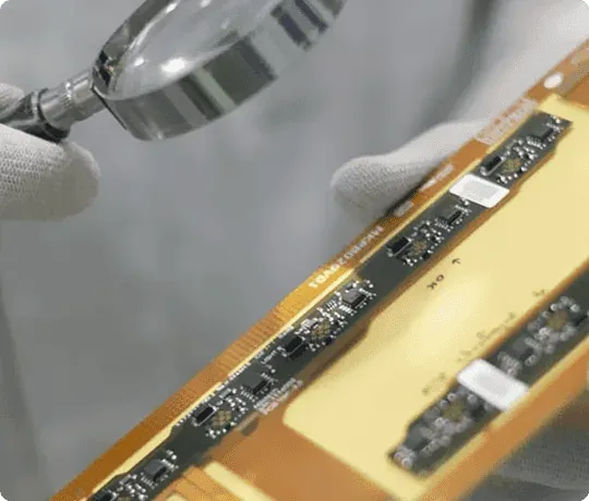
On flex, "construction" is not a drawing layer. It is already bonded into the film.
On a rigid board, construction means the layer order in a stack-up table. Re-press it and you have a new one. Flex does not work that way. Each construction variant — single-sided, double-sided, coverlay openings, local stiffeners — corresponds to a process step that permanently bonds or cures material together. Once it is on, that area's flexibility, machinability and rework options are fixed.
That is the fundamental difference from rigid work: rigid constraints are mostly dimensional windows (can it be made), flex constraints are mostly sequence (can it still be changed afterwards). Every "while we're at it, add a layer" decision an engineer makes is an irreversible action on the shop floor.
This article answers one question: going one step up from single-sided flex, what constraint does manufacturing gain, which process step does it lock into, and why can it not be reversed later. It does not cover routing inside the bend area (see flex conductor routing and bend area rules), does not compare coverlay material grades (see coverlay and polyimide material selection), and does not review stiffener drawing fields (see stiffener drawing review).
> For the board type itself — specification ranges and typical applications — see the flex PCB product page: 1–8 layers, PI base material, 2 mil minimum trace width, bend radius ≥6× board thickness, 0.5oz–2oz copper, PI/PSA coverlay. The product page owns selection. This article owns the manufacturing boundary when construction escalates.
S0 single-sided flex: fewest constraints, and the easiest one to talk yourself into
Single-sided flex has one copper layer, all routing on one face, coverlay on one side. It is the most permissive flex form in manufacturing: no layer-to-layer registration, no through holes, and a bend area that is essentially safe as long as conductors cross it perpendicular.
The real boundary at this level is routing density. The product page gives 2 mil minimum trace width, consistent with the 2/2 mil trace/space on the capabilities page. But the tolerance page also states trace width ±20%. At 2 mil, ±20% means a finished trace can land anywhere in roughly 1.6–2.4 mil. For traces that carry controlled impedance or meaningful current, that relative deviation is not negligible. On a single-sided board there is no second layer to offload to, so every signal and every power path has to fit in this one layer's width budget.
"We'll move to double-sided later if it isn't enough" sounds like a safe plan. It is not: the move triggers all three constraints in the next section at once, which means redoing the construction. Whether single-sided works should be settled against final function in the first revision, not treated as a starting point.
S1 double-sided flex: adds registration and holes, locked at drilling and hole metallization
Adding a second copper layer doubles routing area and adds three constraints in one move, all locked in the front end of the process:
Constraint 1: layer-to-layer registration. The capabilities page gives ±0.025 mm positional accuracy. On rigid boards this describes the relationship between drilling and inner-layer imaging. On flex, the PI film changes dimensionally under tension and under heat and humidity as it moves through the line, so registration is harder than on a rigid board of the same specification. Once registration drifts out, there is no recovery at finished-board stage — the holes are already drilled in the wrong place.
Constraint 2: the through holes themselves. Minimum hole 0.075 mm, hole diameter tolerance ±0.05 mm, aspect ratio ≤10:1 (all from the capabilities page). Flex is thin overall, so aspect ratio is usually not the bottleneck. The bottleneck is where the holes are allowed to go, which leads to the third constraint.
Constraint 3: the bend area stops being a design option and becomes a keep-out. On single-sided flex, the bend area only needs conductors crossing perpendicular. On double-sided flex, a via or pad in the bend area makes that spot a stress concentration. So the practical effect of going double-sided is that it removes the bend area from usable real estate. The complete rule set lives in bend area routing rules; here the point is that this is the structural price of the upgrade, not a detail to optimize separately.
The reason it is irreversible is direct: hole positions and layer registration are fixed at drilling and hole metallization. Coverlay, surface finish and profiling downstream can only accept them. Changing means new material.
S2 coverlay and openings: adds a registration budget, locked at lamination
Coverlay (the product page lists PI/PSA) replaces solder mask and protects conductors while defining solderable areas. It is not printed on. It is a film with pre-cut openings, laminated on, and that difference generates the entire constraint at this level.
New constraint: the opening registration budget, and it stacks two errors. The tolerance page gives solder mask registration ±0.003″, openings 0.003″ larger than the pad (mask swell), standard mask bridge 0.004″, and special handling likely when pad pitch is under 0.010″. A coverlay opening has to absorb the film's own die-cut or imaging error plus lamination placement error, so the usable budget is tighter than rigid solder mask.
The failure goes two ways, both common:
- Opening too small or offset → part of the pad stays covered, solderable area is short, and it only shows up at assembly.
- Opening too large → the film bridge between adjacent pads cannot fit, conductors are exposed, and fine-pitch areas (pad pitch under 0.010″) go straight to special-handling review.
Why it is irreversible: coverlay is laminated and cured. You cannot peel it off and re-place it. A wrong opening scraps that board. This is why coverlay openings have to be confirmed together with assembly pad requirements at DFM stage instead of inheriting rigid solder mask habits.
S3 local stiffeners: what gets added is a permanent no-bend zone
A stiffener is bonded over connector areas, assembly areas or insertion ends to restore local rigidity for mating and placement. What it adds is not a dimensional limit. It is a permanent structural property.
New constraint: bendable area is permanently removed, and the boundary becomes a new stress concentration. Once bonded, that region no longer takes part in bending. The real risk is at the boundary — the line where the stiffened region transitions into free flex is where bending stress concentrates most. The product page gives bend radius ≥6× board thickness, and that radius has to be achieved outside the stiffener boundary, not counted into the area under it.
Why it is irreversible: stiffeners bond through a cured adhesive layer, late in the process. Removing one in rework damages the coverlay and the copper foil with it. The full set of review fields for position, outline and adhesive boundary is in stiffener drawing review. The point here is one thing: a stiffener writes "no bending here" into physical material. It is not an adjustable part.
S4 top of the ladder: when a flex board needs more and more rigid area
If construction has reached "multiple stiffeners + double-sided + many openings + components mostly on stiffened areas", the return on stacking more onto pure flex drops fast. Each stiffener is another bonding step, another stress boundary, another no-rework zone.
At that point the comparison is rigid-flex. The rigid-flex product page gives 2–20 rigid layers, 1–8 flex layers, 3 mil minimum trace width, 0.3–4.0 mm board thickness, FR-4+PI base material, and ≥100,000 bend cycles. Note that its minimum trace width (3 mil) is wider than pure flex at 2 mil: that is the density price paid for structural capability. The four selection criteria are covered in rigid-flex vs flex construction boundaries and are not repeated here.
How to use this ladder
Treat it as a one-time classification, not an incremental upgrade path:
| Level | Constraint added | Locked at | Reversibility |
|---|---|---|---|
| S0 single-sided | Width budget (2 mil with ±20% trace tolerance) | Etching | Reversible by revision |
| S1 double-sided | Registration ±0.025 mm, hole positions, bend area keep-out | Drilling / hole metallization | Irreversible, needs new material |
| S2 coverlay openings | Stacked registration budget (±0.003″ class) | Lamination | Irreversible, error scraps the board |
| S3 stiffener | Permanent no-bend zone + boundary stress | Bonding / late profiling | Irreversible, removal damages the part |
| S4 → rigid-flex | Density price (3 mil minimum trace) | Whole-structure redefinition | Change of board type |
All ranges come from published SKPCB pages. Both the product and capability pages state that the listed windows are not universal commitments for every product, so the feasibility of a specific combination must be confirmed in engineering review.
Four things to submit together for review
Structural classification cannot be judged from one drawing. These four have to arrive together, or the package gets returned for more information:
- Structural intent: which areas bend, formed once or cycling in service, bend radius and direction (checked against ≥6× board thickness).
- Layer count and copper combination: single- or double-sided, which copper weight in the 0.5oz–2oz range, and the finest trace width actually required with that combination.
- Coverlay opening requirements: which pads open, the minimum pad pitch (whether it reaches under 0.010″), and whether any fine-pitch connector areas are involved.
- Stiffener intent: position, outline, assembly side, and the distance from the stiffener boundary to where bending starts.
To open a project-level review, submit data from the flex PCB product page or go directly through the quote entry. Capability windows are on the capabilities page and tolerance definitions on the tolerance page.
FAQ
Can a single-sided flex be converted to double-sided later?
Technically yes, but that is not a conversion, it is a rebuild. Double-sided introduces registration, hole positions and a bend-area keep-out simultaneously, so bend area that was usable may no longer be, and routing has to be redone. Settle single-sided against final function in the first revision.
Can coverlay openings use the same rules as rigid solder mask?
Not directly. The tolerance page figures — registration ±0.003″, opening 0.003″ larger than the pad, standard bridge 0.004″ — are the baseline, but coverlay is a laminated film that also absorbs die-cut and placement error, so the real budget is tighter. Fine-pitch areas (pad pitch under 0.010″) need their own review.
Why can't a wrong coverlay be reworked?
Coverlay is laminated and cured into the base material; there is no non-destructive removal step. A misplaced opening that covers a pad, or a bridge that will not fit, scraps the board. That is why openings are confirmed at DFM stage rather than inspected afterwards.
Can stiffeners be decided after prototyping?
Not advisable. Stiffeners determine which areas can never bend, which in turn changes bend area location, routing layout and coverlay opening boundaries. Adding them after prototypes usually means rearranging the first three levels.
Bend radius ≥6× board thickness — measured from the stiffener boundary or the board edge?
From the free flex section that actually bends. Area covered by a stiffener does not count toward bend length. Counting the radius into the region under a stiffener is a common error and turns the stiffener boundary into a stress concentration.
When should a design go rigid-flex instead of adding more stiffeners?
When rigid regions grow into the primary load-bearing and assembly areas. Continuing with stiffeners at that point simulates rigid-flex construction with several irreversible bonding steps, but you also have to accept the rigid-flex density price (3 mil minimum trace, wider than 2 mil on pure flex). The four criteria are in the rigid-flex vs flex article.
Can these ranges go straight into my specification?
Not as-is. Both the product and capability pages state the listed windows are not universal commitments for every product, and feasible combinations must be confirmed against project data. Use them as screening boundaries; final values come from engineering review.