In most projects, surface finish gets decided like this: the stack-up is settled, the hole types are settled, the depanel method is settled, assembly flow is planned, and then someone asks, just before release, "what do we put down for surface finish?"
That sequence is the problem. Not because it is too late to change anything, but because by the time the question is asked, the option set has already been filtered by all those earlier decisions — and nobody recorded the filtering. The selection discussion then becomes a comparison among leftover options, while everyone in the room believes they are choosing from the full set. The question that should be asked first is: what does this board's structure still allow?
Our existing surface finish comparison answers what each finish offers and where it fits. ENIG nickel-gold thickness and black pad control answers how one finish is controlled internally. This article answers the step before both: what structure already took off the table.
1. The option set starts shrinking the moment the stack-up is fixed
Surface finish sits late in the manufacturing route, which creates an illusion: that the decision can also sit late.
But process order and constraint order are different things. Surface finish is one process shared by the entire board — the same chemistry, the same pass, serving every pad and structure on the panel simultaneously. Its constraints therefore do not come from itself; they come from whichever structure on the board is hardest to serve. Each structure designed in adds one requirement, and as requirements accumulate the intersection narrows.
The logic mirrors manufacturing tolerances: tolerance is not measured at the end, it is determined by the stack-up and route from the start. Surface finish is not chosen at the end either, it is bounded by structure from the start.
2. The four filters
Structure constrains surface finish through four things. These are not "factors to consider" — they are filters. What does not pass does not pass, and no amount of process skill compensates.
Filter 1: board thickness and warp behaviour. On the finishing line a board is racked, immersed, sprayed and dried. Very thin and very thick boards behave differently through that sequence. Thin boards are vulnerable to deformation and handling marks, which limits which routes involving hot immersion or aggressive spray are usable. Thick boards carry thermal mass that makes uniform processing harder, which limits which routes depending on short, even reactions are usable. This filter is the most frequently missed, because designers treat thickness as an electrical and mechanical parameter rather than a finishing parameter. See also finished thickness tolerance control — thickness is not merely a dimensional outcome.
Filter 2: hole types and edge structures. This is the hardest filter. Castellated holes, gold fingers, blind and buried vias, plated board edges — what they share is that the surface needing treatment is not on the board plane; it is on a cut face or deep inside a hole.
- A castellated hole's copper face is a cut cross-section exposed by routing. It only fully exists after depaneling, while the finish was applied before depaneling. So "how is that ring of copper protected" is necessarily a design question, not a process question. Structural constraints are covered in the castellated holes design guide.
- Gold fingers must survive insertion wear. The property they need is not the property a surface-mount pad needs, which leads directly to the two-finishes-on-one-board requirement (next section).
- Blind, buried and deep holes raise a solution-exchange problem: the deeper and narrower the hole, the harder exchange and drying become, and the narrower the route choice.
Filter 3: whether one board needs two finishes. When a board carries both "to be soldered" and "to be mated" areas, or both "must be very flat" and "must survive repeated thermal shock" areas, a single finish may not suffice. This is not preference; two classes of property are physically difficult for one deposit to provide at once. Once this requirement holds, the option set jumps from "pick one finish" to "pick a combination plus an implementation route" — and combinations are far less feasible than single choices.
Filter 4: the number of downstream thermal cycles. How many high-temperature passes will the board see: single-side reflow, double-side reflow, or reflow plus wave plus rework? Each cycle consumes the state of the interface between deposit and copper. Boards with many cycles bias toward routes that stay reliable after repeated heating; boards with few cycles and a settled assembly flow have a much wider set. The catch is that this information usually sits with the assembler while the finish is decided at the PCB shop — information and decision rights are separated, which is why this filter is the one most often dropped. For the process relationship on double-sided assembly see second-side reflow assembly on double-sided boards.
3. Two finishes on one board: three routes and what each costs
Once filter 3 holds, one of three routes must be chosen. They are not variations in degree — they are three engineering arrangements whose costs land in completely different places.
Route A: selective finishing with local masking. Apply one finish across the board, mask the areas that should not receive the second, then apply the second locally. The cost lands on masking accuracy and boundary definition: there will always be a transition band between the two finishes, and its position and width must be defined on the drawing, or it will end up somewhere you did not intend. Masking is also an added process step, increasing route length and the chance of rework.
Route B: sequential processing ordered by process window. Both finishes are applied over large areas, with differentiation coming from process order and mutually incompatible chemical windows. The cost lands on irreversibility once the order is set: the later process must not destroy the result of the earlier one, which compresses feasible combinations to very few.
Route C: separate the two areas structurally. Do not solve it on one board. Change the design — make the mating portion a separate part, switch to a connector, or change the depanel approach so the two area types land on different boards. The cost lands on design and BOM, but it is the only one of the three that adds no process uncertainty.
The recommended order of engineering judgement is C → A → B: first ask whether coexistence can be avoided; if not, look at local masking; only then consider forcing it through process sequence. In real projects the order is usually reversed — coexistence is assumed mandatory and then a process workaround is sought, which pushes a problem into the factory that design could have absorbed.
4. Which combinations are mutually exclusive
Some combinations are not "difficult"; they do not hold. You identify them not from a table but from three conflict points:
- Flatness versus wear resistance. Fine-pitch areas demanding extreme flatness and contact areas demanding repeated-insertion durability want opposite things from a deposit: thin and uniform versus thick and wear-resistant. One deposit cannot optimise both, which is the entire reason routes A and B exist.
- Chemical compatibility. Will the later process's chemistry attack the already-formed surface of the earlier one? This conflict defines the few feasible orders for route B, and also makes certain "both finishes, full board" requirements simply unachievable.
- Coverage accessibility. Can the surface needing treatment be physically and evenly reached by the chemistry? Deep narrow holes, cut faces exposed only after depaneling, and areas shadowed by components or hardware fall here. This conflict cannot be solved by switching finish type, only by changing structure — which is why filter 2 is the hardest one.
A related failure, not exclusivity but equally fatal: solder mask openings and surface finish coverage not aligned. This is sharpest on heavy copper, see heavy copper solder mask and surface finish coverage. The mask opening defines which copper gets treated; get the opening wrong and a correctly executed finish still lands in the wrong place.
5. Where in the flow this question belongs
The answer: at the stack-up review, not before release.
More precisely, four nodes each owe one piece of surface finish information:
| Node | Information owed | Consequence if missing |
|---|---|---|
| Requirements definition | Downstream thermal cycle count, presence of mating contacts, service environment | Inputs for filters 3 and 4 are absent, so selection becomes guesswork |
| Stack-up and thickness review | Board thickness and allowable deformation | Filter 1 surfaces after release, possibly forcing a stack-up change |
| Hole and edge structure review | Presence of castellations, gold fingers, blind/buried vias, plated edges | Filter 2 surfaces at manufacturing, when structural change is most expensive |
| Depanel method review | Whether depaneling creates new bare copper cut faces | Castellation-class problems get pushed past delivery |
With those four in hand, the viable set is usually down to two or three finishes. Only then does comparison of merits begin — and that is exactly where most selection discussions actually start, mistaking it for the starting line. Read our manufacturing capabilities page alongside those four items: capability states what we can produce, the four items state what your board allows, and the intersection is the real option set.
6. What the drawing must say to be executable
A single line — "Surface finish: ENIG" — is sufficient when there is one finish and no special structures. The moment any of the four filters is active, it is not. An executable drawing adds:
- The applicable area of each finish, not just its name. With two finishes, boundaries must be drawn or identified on a layer. Text saying "hard gold on the gold finger portion" is not enough; the factory cannot infer where "the portion" ends.
- Allowed position and acceptable condition of the transition band. State the acceptable range for appearance and location of the band between two finishes up front, or it becomes a dispute later.
- Requirements for cut faces and edge structures. For copper exposed only after depaneling, state the expected condition and whether that expectation is achievable in the current route — sometimes the correct answer is to accept bare copper and handle it on the assembly side.
- A declaration of downstream thermal history. State how many high-temperature passes the board will see. This is a direct input to route selection; without it the shop must assume the most common case.
- Explicit no-substitution notes where applicable. If a finish cannot be substituted, say so. Otherwise, when a structural conflict appears, an equivalence-based substitution may be applied that happens to break your assembly premise.
These items belong to the same layer of work as the multilayer stack-up release checklist: turning design intent into instructions manufacturing can execute directly, rather than descriptions requiring clarification rounds. Our surface finish page lists common options and applications, and as that page states, the final choice still follows from drawing, material and downstream process — which is, in substance, the four filters described here.
7. Summary: get the order right and selection is not hard
Surface finish selection turns into a tug-of-war not because finish properties are hard to understand — that material is abundant. The difficulty is that it sits in the wrong place in the flow: placed last, you can only choose among leftovers, and since no one recorded which earlier step closed which option, the discussion has no shared premise.
Move it to the stack-up review, make the four filters' inputs a review deliverable, and the selection conversation gets much shorter without forcing structural rework after release.
FAQ
Q1: The board is already designed and we are only now thinking about surface finish. Is it too late?
Not too late, but the viable range may be narrower than you expect. Walk your design against the four filters above and you will quickly see which options are already closed. If the finish you want conflicts with a structure, the choice is change the structure or change the finish — and the earlier that judgement is made, the cheaper it is.
Q2: Why not simply always pick the best finish?
Because no finish is optimal on every axis; "best" depends on which structure on the board is hardest to serve. More importantly, some structures make an otherwise well-suited finish unachievable (the coverage-accessibility conflict in filter 2), and in that case "best" is not available.
Q3: Is two finishes on one board expensive?
What it adds is mainly route length and uncertainty rather than deposit cost: one more masking step or one more pass means one more variation source and one more rework possibility. That is why this article suggests first asking whether coexistence can be avoided at all (route C). Real quoting needs the drawing and area definition; it cannot be estimated from finish names.
Q4: What is the actual answer for surface finish on castellated boards?
The key realisation is that the castellated copper cut face only fully exists after depaneling, while the finish was completed before it. So this is not a question of which finish, but of what condition the cut face is expected to be in, whether that expectation is achievable in the current route, and who absorbs it when it is not. Settle the structure first with the castellated holes design guide, then discuss finish.
Q5: Thermal cycle count is information only our assembler has. Should it go on the drawing?
Yes. Of the four filters, this is the only input that naturally sits with neither the designer nor the fabricator but with the assembler. Without it the PCB shop must assume the most common case, and a wrong assumption only shows up at assembly, when the boards are already built.
Q6: How are surface finish and solder mask related, and why do you keep raising mask openings?
Because the mask opening defines which copper the finish reaches. Get the opening wrong and the finishing process can be executed perfectly while treating the wrong areas. The two must be reviewed together; the coupling is most visible on heavy copper, see heavy copper solder mask and surface finish coverage.
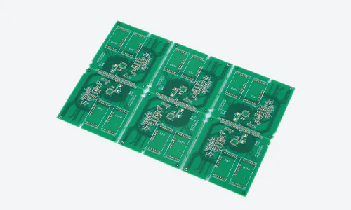
Cover image alt: Angled view of a bare printed circuit board panel with green solder mask, six identical boards in a two-by-three array joined by retained breakaway tabs along routed outlines; the surface shows white silkscreen, silver-white pads, one long row of fine-pitch connector pads, multiple rectangular and square surface-mount pad sites, oval pads, and plated holes distributed across the boards and along their edges.
---