Multi-Layer Stackups
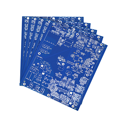
As a guideline, below are the standard stack-ups used by Bay Area Circuits for both our 4 layer PCBs and 6 layer PCBs with a .031 or .062 overall thickness*. 4 and 6 layer PCB stackups are not guaranteed unless a specific stackup is identified in Gerber files and/or fabrication drawing/notes.
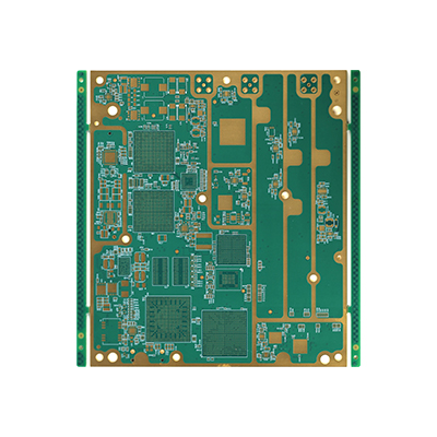
For different standard PCB thickness, higher layer counts, or designs requiring controlled impedance or controlled dielectric, please contact us for more information. We’ll be glad to review your impedance requirements and adjust the stack-up accordingly.
Defined layer buildup
Prepreg thicknesses after pressing, at approx. 80% copper utilization on the inner layers
Defined layer buildup - 4 layers:

Defined layer buildup - 6 layers:

Defined layer buildup - 8 layers:


