


Products
Multi-Layer PCB
- Layers
- 4-40 layers
- Board Thickness
- 0.4mm - 6.0mm
- Min. Trace Width/Space
- 3mil/3mil
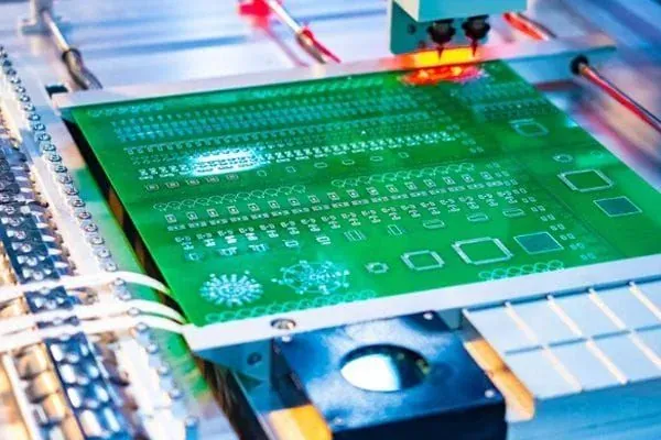
Relevant production base
SUNKING JI AN CIRCUITS ELECTRONICS CO., LTD.
Technical Specifications
| Specification | Value |
|---|---|
| Layers | 4-40 layers |
| Board Thickness | 0.4mm - 6.0mm |
| Min. Trace Width/Space | 3mil/3mil |
| Min. Finished Mechanical Hole | 0.15mm |
| Impedance Control | ±5% (±10% std) |
| Base Material | FR-4/High-Frequency Materials |
Product Features
- 4-40 layers available
- Precise impedance control
- High-density interconnection
- Blind/buried via technology
- High Tg materials
- Excellent signal integrity
Applications
Telecom Base Stations
Server Motherboards
Networking Equipment
Medical Devices
Aerospace
High-End Consumer Electronics
Multi-Layer PCB Product View
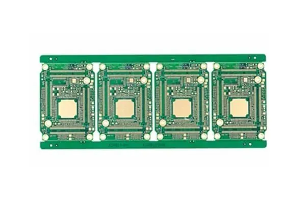
The image shows the panel appearance of a PCB explicitly identified as an eight-layer board on the source page. Appearance alone does not verify its internal stack-up, materials, impedance or electrical performance; project stack-up and inspection data govern.

FAQ
What is the maximum layer count?
- Standard PCB production up to 40 layers; IC substrates up to 64 layers.
What is the impedance control tolerance?
- Standard impedance control is ±10%, with high-precision options at ±5%.
What special processes are supported?
- We support blind/buried vias, back drilling, resin plug, step boards and more.
Related Products


Related Technical Articles


Need a quote for Multi-Layer PCB?
Upload your Gerber files and we'll quote within 1 hour for simple boards, 24 hours for complex builds.
Get Quote Now