Heavy Copper PCBs
High-quality, quick-turn heavy copper PCB fabrication services
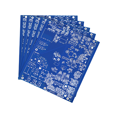
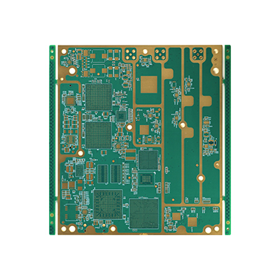
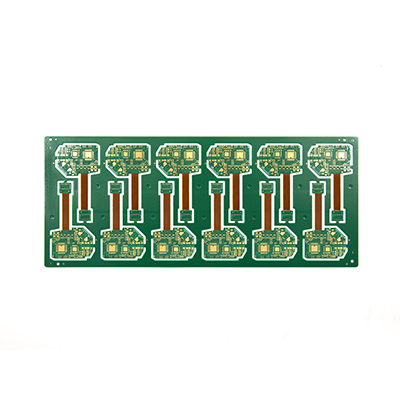
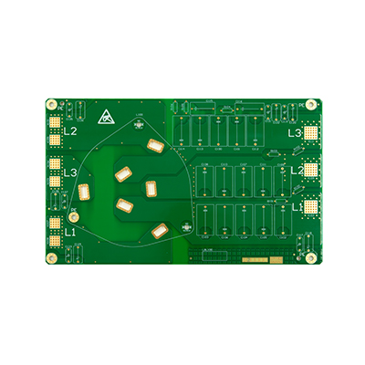
High-Quality Heavy Copper PCB / Thick Copper PCB
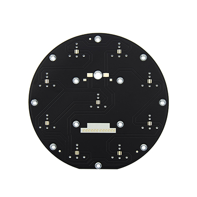
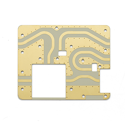
If you keenly follow the electronic industry’s latest trends, you might have heard of heavy copper PCBs. They have found their way into various applications because of their numerous benefits. Though they are a bit expensive to fabricate, their value exceeds the expenses.
Thick copper PCBs have finished copper weights of over 4oz (140μm), compared to the 1oz (35μm) and 2oz (0μm) copper weights typically found in standard boards. The extra copper thickness allows the PCB to carry more power, establish high thermal circulation, and perform complex switches in a small space.
SUNKING is several miles ahead of other PCB service providers in providing a wide variety of thick copper PCBs. These boards are available in different ranges and models as per the industry standards and customer specifications. Our products undergo a rigorous quality inspection process to guarantee the delivery of defect-free PCBs.
Our Heavy Copper PCB Quality Inspection Procedure
At SUNKING, we are obsessed with quality, and we always aim for a flawless design and functionality of our thick copper PCB products. We have laid out a 5-step quality inspection procedure to ensure our products are 100% functional:
Benefits of Heavy Copper PCBs
The thick copper facilitates heat transfer to the external heat sink and conveys a higher current. This is made possible with the integration of plated vias. Thick copper
PCB can support high current frequency, repeated thermal cycling, and high temperatures.
They minimize the chances of experiencing circuit failures.
Thick copper boards have high resistance to thermal strains.
They display compact sizes with various copper weights.
Its PTH holes and connector sites display high mechanical power.
Thick copper PCBs can transmit heavy current.
They come with exotic materials for improving the PCB’s mechanical features.
They eliminate complex wire bus configurations.
Applications of Heavy Copper PCBs
Heavy copper boards display a high elongation performance and are not limited by the working temperatures. They are commonly used in hot-melt welding equipment and severe corrosive atmospheric conditions. Below is a comprehensive list of thick copper PCB applications.
Reliable performance and good thermal dissemination are the main factors driving the high
demand for thick copper boards. The modern printed circuit boards are designed to conduct
high current, meaning a lot of heat is generated. But, thick copper PCBs help to disseminate
the generated heat quickly.This ensures the optimum performance of a product.
HVAC systems
Power line monitors
Solar power converters
Power converters for railway electrical systems
Nuclear power applications
Protection relays
Welding equipment
Safety and signal systems
High power rectifiers
Torque controls
Power supplies for radar systems
Excitation systems for power regulators

